Well, here's page one of my homebrew stuff. I haven't taken photos of my gear
yet but here's a few projects I've done.
- Reverse-engineered the TLM103 amplifier. It's clever.
- Upgraded an Apex 430 microphone's amplifier, transformer, and capsule.
Really, rebuilt the whole mic...
- Rebuilt an Apex 460 microphone. New capsule, transformer, and removal of
the cathode follower stage. It doesn't need it if the transformer is correct.
- Built from scratch a CK61-ULS based tube mic. It needs a quieter tube but
it works. I'm using a 5744 tube.
- Designed an upgrade for the Oktava mic's. It emulates the C61 system where
capsule bias is obtained via the cathode load. Check out the photo...
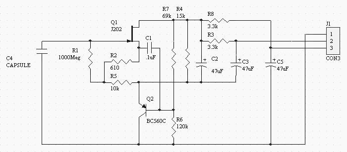
R1 feeds bias voltage to the capsule and to the JFET Q1. R2 sets the
quiescent current of Q1. R5 is set to adjust the voltage drop across Q1, but is
typically about 10k. R4 feeds additional current to Q2. Note that Q1's current
is also reused by Q2 just like in the original Oktava circuit. R7 and R6 set the
nominal DC output voltage. Note that the buffered output signal is applied to
pin 2 (the ouput) but also via C2 to the power supply of Q1. This tends to
reduce gate-channel voltage modulation by forcing an (approximate) DC voltage
across Q1, as well as lowering Q1's output impedance. C5 is the familiar
pseudo-balanced output grounding capacitor. To improve cable noise rejection,
series resistors of 49 ohms in line with pins 2 and 3 of the XLR connector may
be a wise idea. To do even better, the resistor in series with pin 3 should be
matched to the output impedance of the amplifier. I have not tested this circuit
yet, but simulations show it works well. The next run of PC boards I do will
have this design on it as a replacement PC board for the Oktava MC012.
Dale's philosophies on condensor mic preamps:
- the simpler circuits don't perform as well technically but they tend
to give a certain character to the sound. If we wanted microphones that
perform technically well, B&K (DPA) or Earthworks measurement mics would be
all we would ever use. The U47 has a lot of distortion and anything but a flat
frequency response. But they sound good.
- Frequency response isn't everything. Frequency and phase response and
distortion characteristics need to be all considered. Remember that the output
of most mic amplifiers (the one or two transistor kind, or glass, for that
matter) is fed back capacitively to the input. Any distortion or frequency
response anomalies in the mic amplifier are re-applied to the input of the
amplifier but also to the electro-mechanics of the capsule. It seems pretty
obvious but I never see a phase plot of a microphone in a data sheet, let
alone real distortion characters. But separating out each component and
duplicating each component (frequency, phase, and distortion) may not result
in 'the sound'. This sort of transfer function may also be non-reversible. If
you know the output you may not be able to get the input that accurately.
- 'The magic' isn't magical at all. Take the U47, for example. Its sound has
a magical quality to it, yes. But that magic is predictable. Start with the
shape and size of the body, mesh size and air volume around the capsule, the
capsule itself, and all of the real amplifier characteristics. Add the
magnetic characteristics of the output transformer and the inevitable coupling
between the magnetic leakage of the output transformer and the amplifier tube
located directly above it.... if you really analyze the system carefully
you'll find the 'magic'. It ain't voodoo, folks. If you take the time to
really analyze what the system is doing you find the answer. That's not to say
you need to but you can't just dismiss things as magic or unpredictable or
unrepeatable. If you really wanted to, you could clone the sound of a U47.
